Apr 12 2010
Imagine the impact on the lighting design industry—and life as a consumer of lighting—if there was a flexible, energy-efficient, paper-thin light source that could be produced economically.
 GE and Konica Minolta to show the world's first general-lighting quality flexible OLEDs. Presenting application ideas during two industry trade shows this year, Light + Building 2010 in Frankfurt, Germany and LightFair 2010 in Las Vegas, Nevada, USA
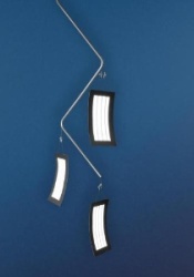
GE Lighting (NYSE:GE) will preview potential organic light-emitting diode (OLED) lighting application ideas during two industry trade shows this year, Light + Building 2010 in Frankfurt, Germany and LightFair 2010 in Las Vegas, Nevada, USA. The company will show OLEDs in a number of configurations at both shows, including fixture prototypes that help to demonstrate the expected competitive advantages of GE’s approach to OLEDs: flexibility and an ultra-thin form factor.
“Lighting is becoming more than just a functional, utilitarian aspect of an environment,” says Zoltan Vamos, GE Lighting’s Budapest-based global general manager of lighting technology. “We’re still experimenting and imagining a future with OLEDs but we think our approach will allow us to apply light to literally any surface at a thickness of just a few sheets of paper.”
“OLED technology represents the biggest potential for new product development and advances in the lit environment,” comments Simon Fisher, director of product design with LAPD Lighting Consultants, Lemsford Village, Hertfordshire, UK. “The potential contained within flexible thin film lighting is enormous and holds the key to changing the way we design and coordinate lighting into our architecture and environments.”
According to Sheila Kennedy, AIA, principal of Kennedy & Violich Architecture, Ltd., “OLED technology presents a new material for lighting that appeals to our senses, our creativity and our environment. Imagine an energy efficient, flexible white light that can be produced with a very low-carbon manufacturing footprint and can be designed to bend into lightweight, luminous forms or be integrated into the surfaces of architecture. With flexible OLED materials, GE has the potential to re-invent the fundamental form and industrial ecology of the light bulb.”
Researchers and product development teams from GE Lighting in Cleveland in partnership with Konica Minolta Holdings, Inc., Konica Minolta Technology Center, Inc. (collectively KM) and GE’s Global Research Center in Niskayuna, New York, have been working together on OLED technology since 2007. GE’s technology partnership with KM, a world leader in imaging products, has enabled GE engineers to tap into KM’s thin-film technology, which plays an important role in the development of highly productive OLEDs.
“The time is right for OLEDs to emerge as an option for consumers, as new energy regulations taking hold around the world are impacting the design, use and disposal of lighting products,” notes Vamos. “OLEDs are a gateway to limitless design possibilities that can keep pace with protocols today and anticipate those yet to come.”
GE has worked with a number of prominent lighting designers, architects and graphic designers, including Fisher and Kennedy, to ensure its early OLED solutions can be used in real-world scenarios. OLED solutions produced as GE and KM envision hold promise for lowering the costs to produce, use and maintain lighting. GE’s OLED solutions will be mercury-free, lightweight and dimmable.
What are OLEDs?
OLEDs are thin, organic materials sandwiched between two electrodes, which illuminate when an electrical charge is applied. In addition to widespread design capabilities, OLEDs have the potential to deliver dramatically improved levels of efficiency and environmental performance, while achieving the high quality of illumination found in traditional light-emitting diode (LED) systems.
KM was the first company to develop proprietary blue phosphorescent materials. In 2006, KM combined this material with multi-layer film design and innovative optical design technologies to successfully develop white OLEDs. KM’s experience making photosensitive materials and coatings has enabled the development of a highly productive roll-to-roll coating process using advanced barrier films that are considered indispensable for prolonging the life of OLED lighting. This approach, similar to newspaper printing, is expected to be less costly than the common evaporation method that forms films one by one on glass substrate. The few organic electronic products on the market today are made with more conventional batch processes and are relatively high in cost.
KM sees OLED lighting as one of its most promising new businesses. It began the construction of a new pilot line in November 2009 to establish a mass production capability. The line will be completed in the autumn of 2010. A roll-to-roll manufacturing infrastructure that enables high performance and low cost devices will allow a more widespread adoption of GE’s OLEDs when commercialization of the product—various sized panels of light (based on 75-mm X 150-mm or 3-inch x 6-inch)—starts in 2011.
Source: http://www.ge.com